rz80 builds

The Z80 core of rejunity/z80-from-schematics on every ASIC PDK and FPGA board, from the latest Targets run on main where all of them passed: main @ bfdb6a9, published 2026-11-13 05:22 UTC.

ASIC chip layouts

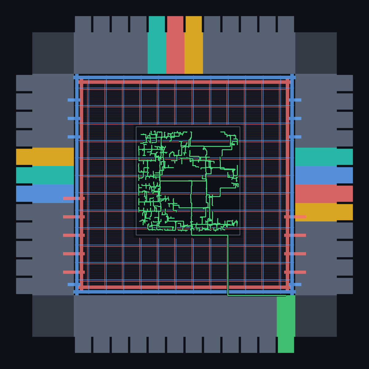
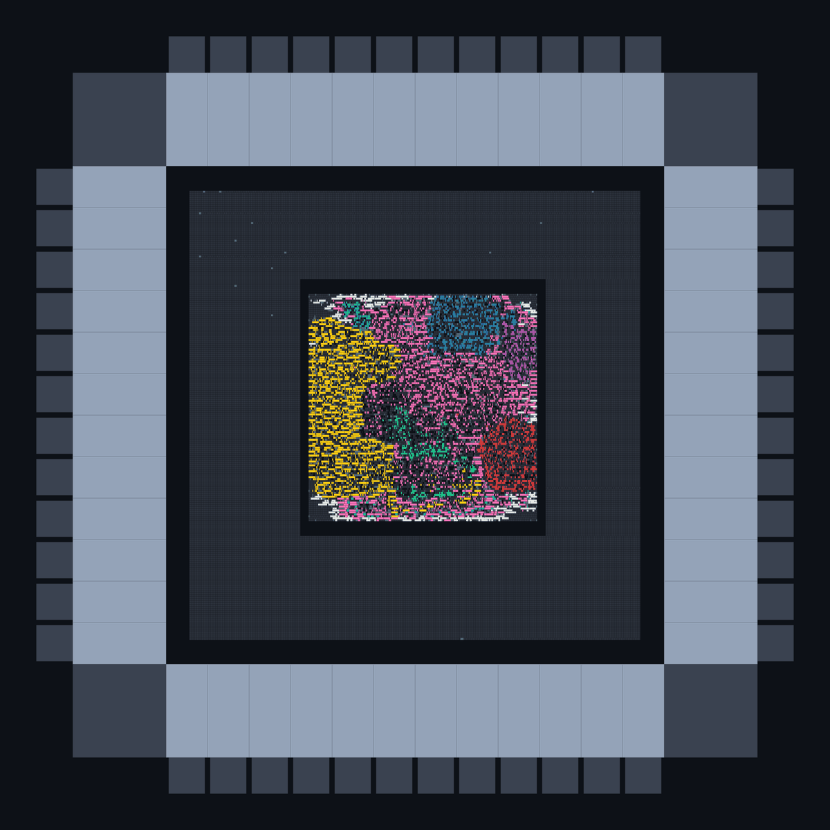
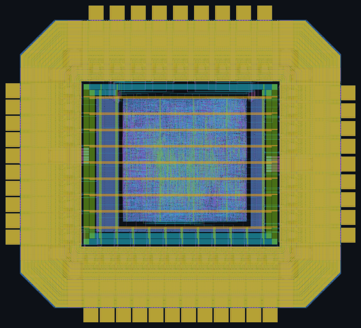
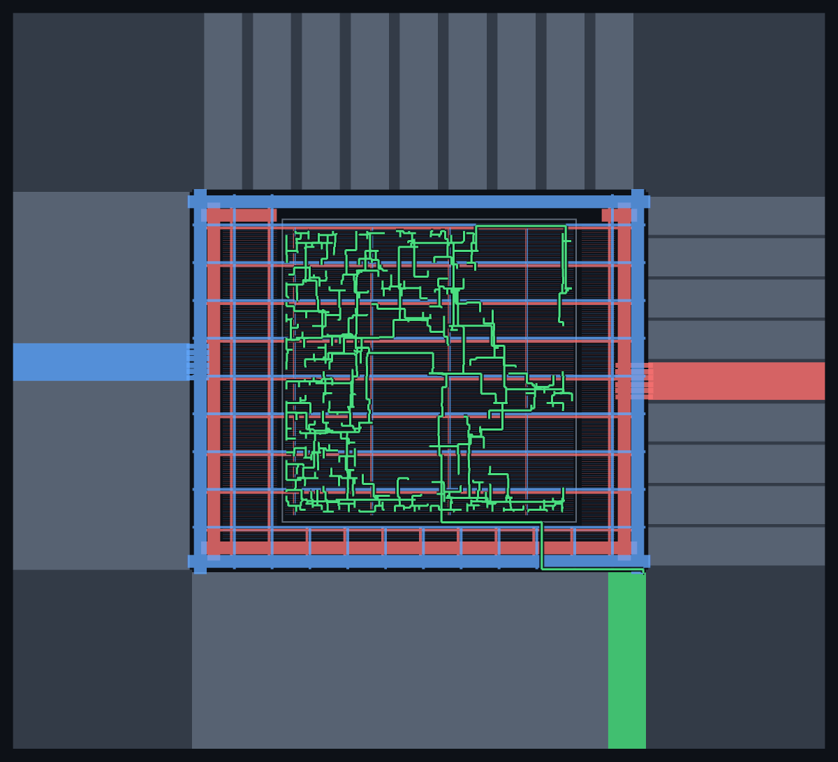
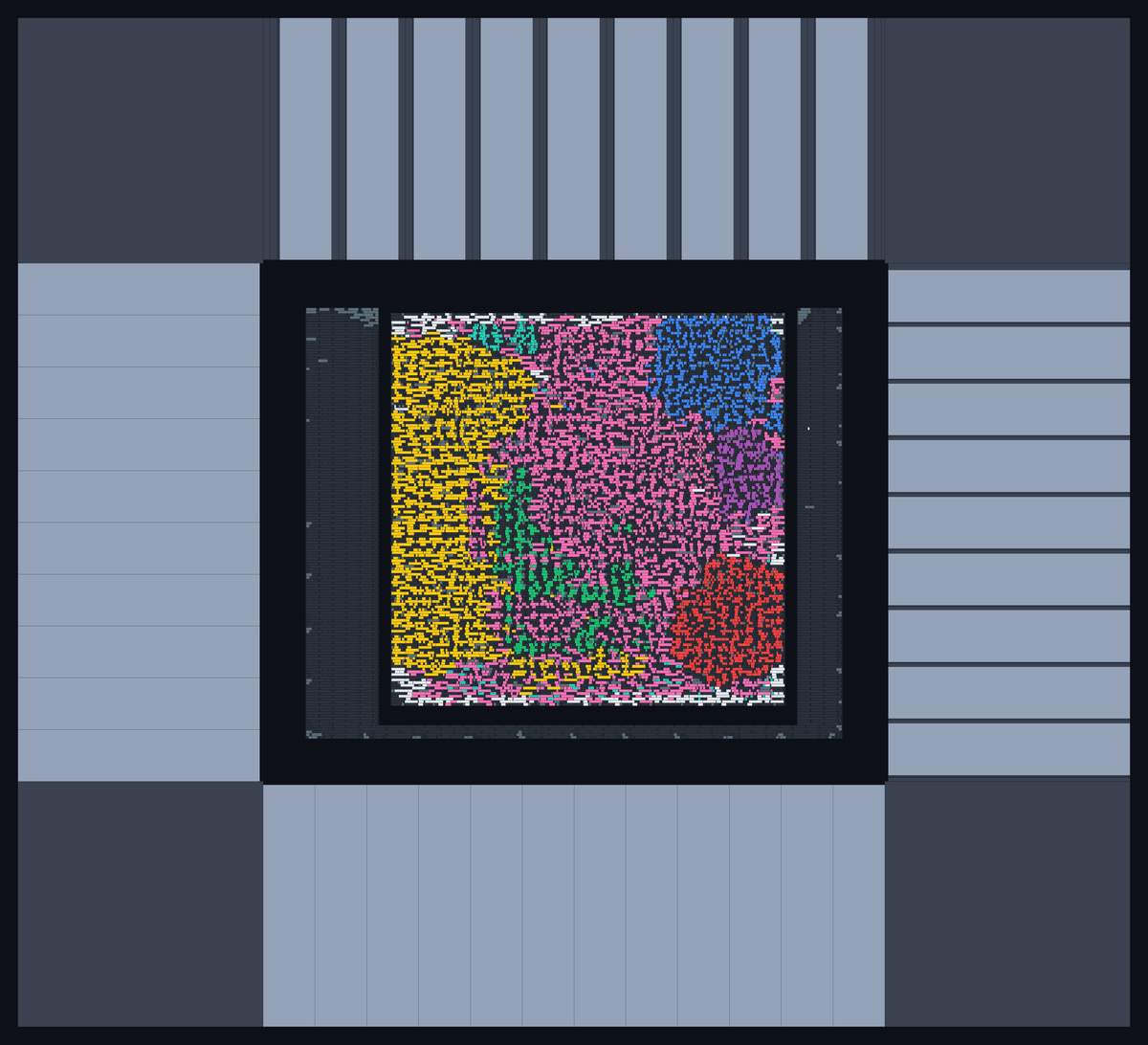
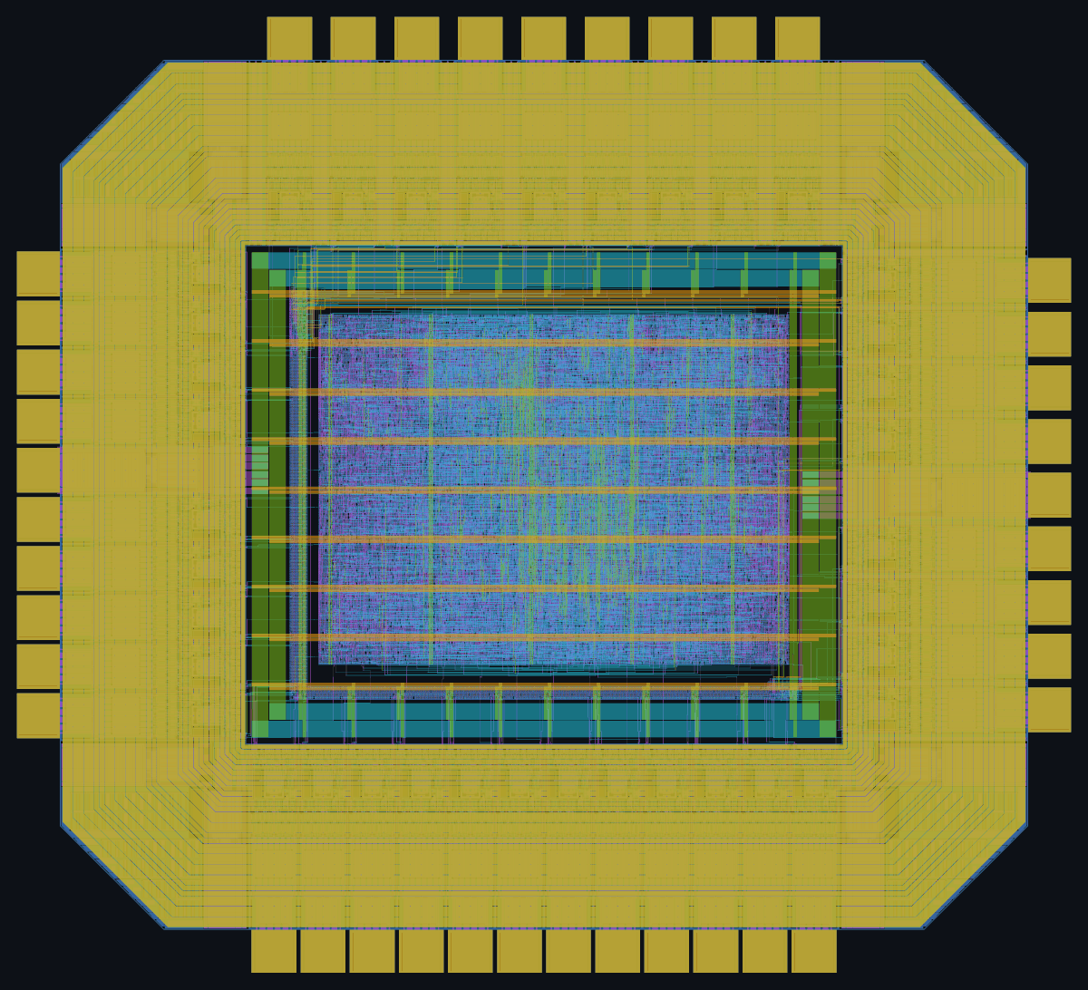
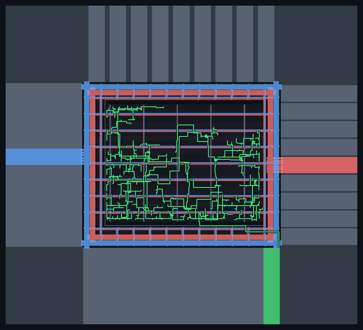
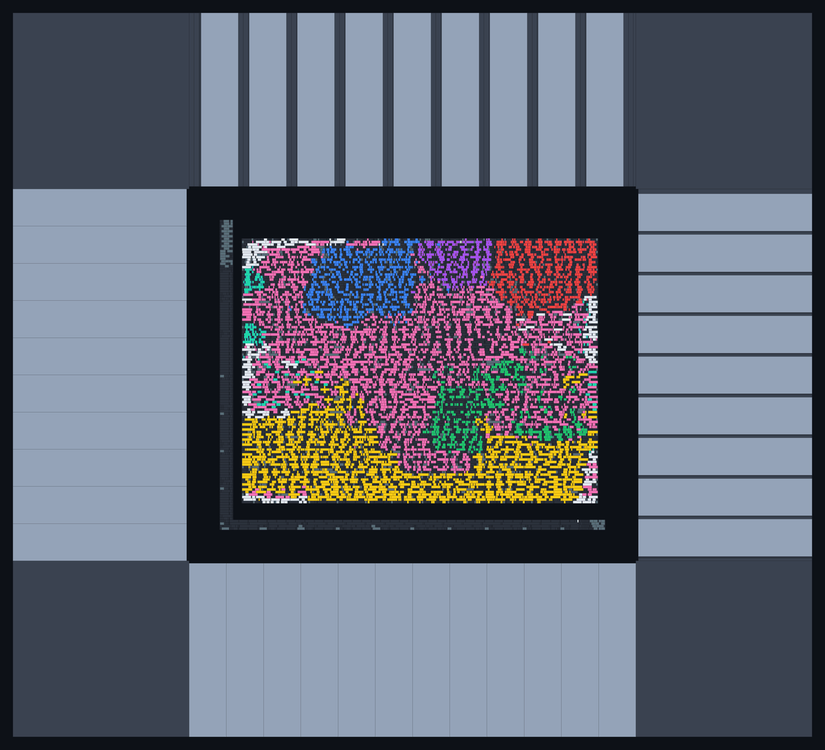
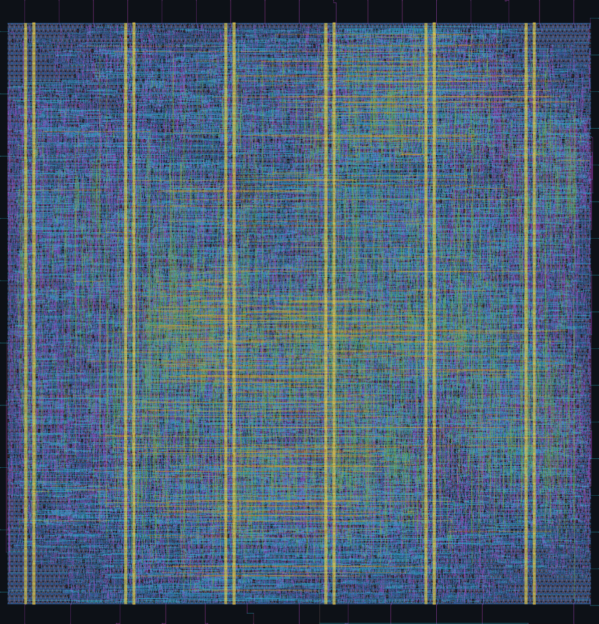
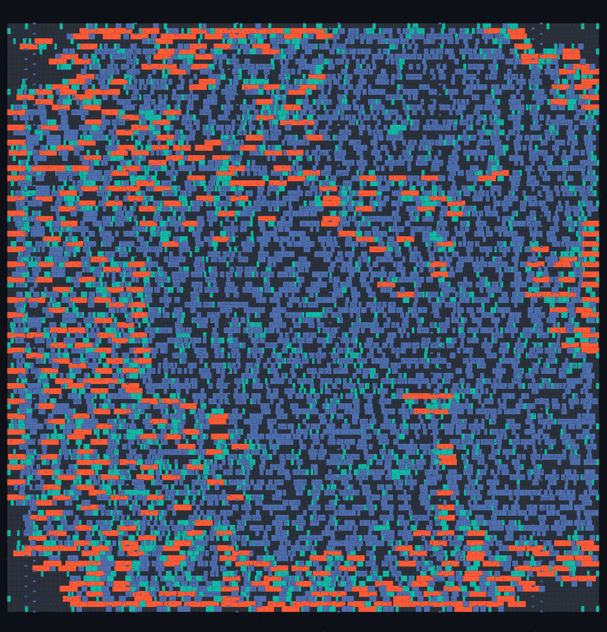
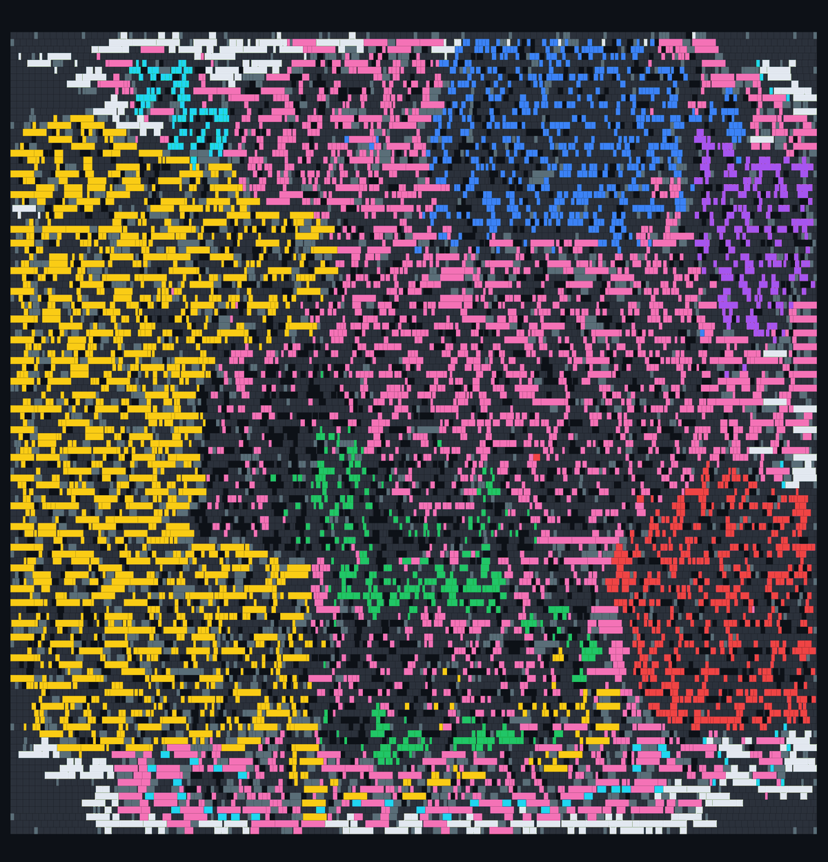
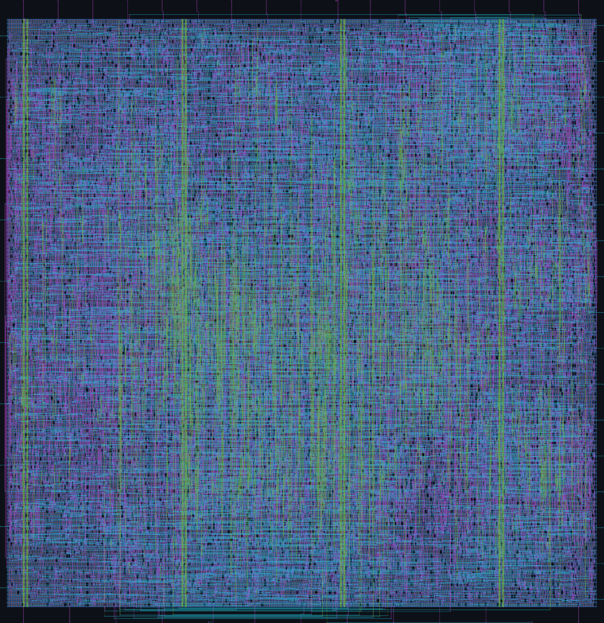
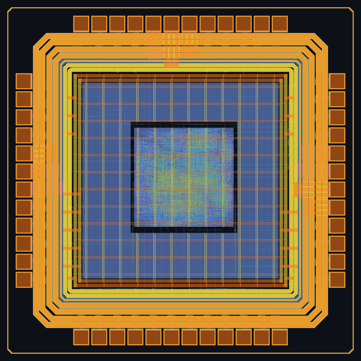
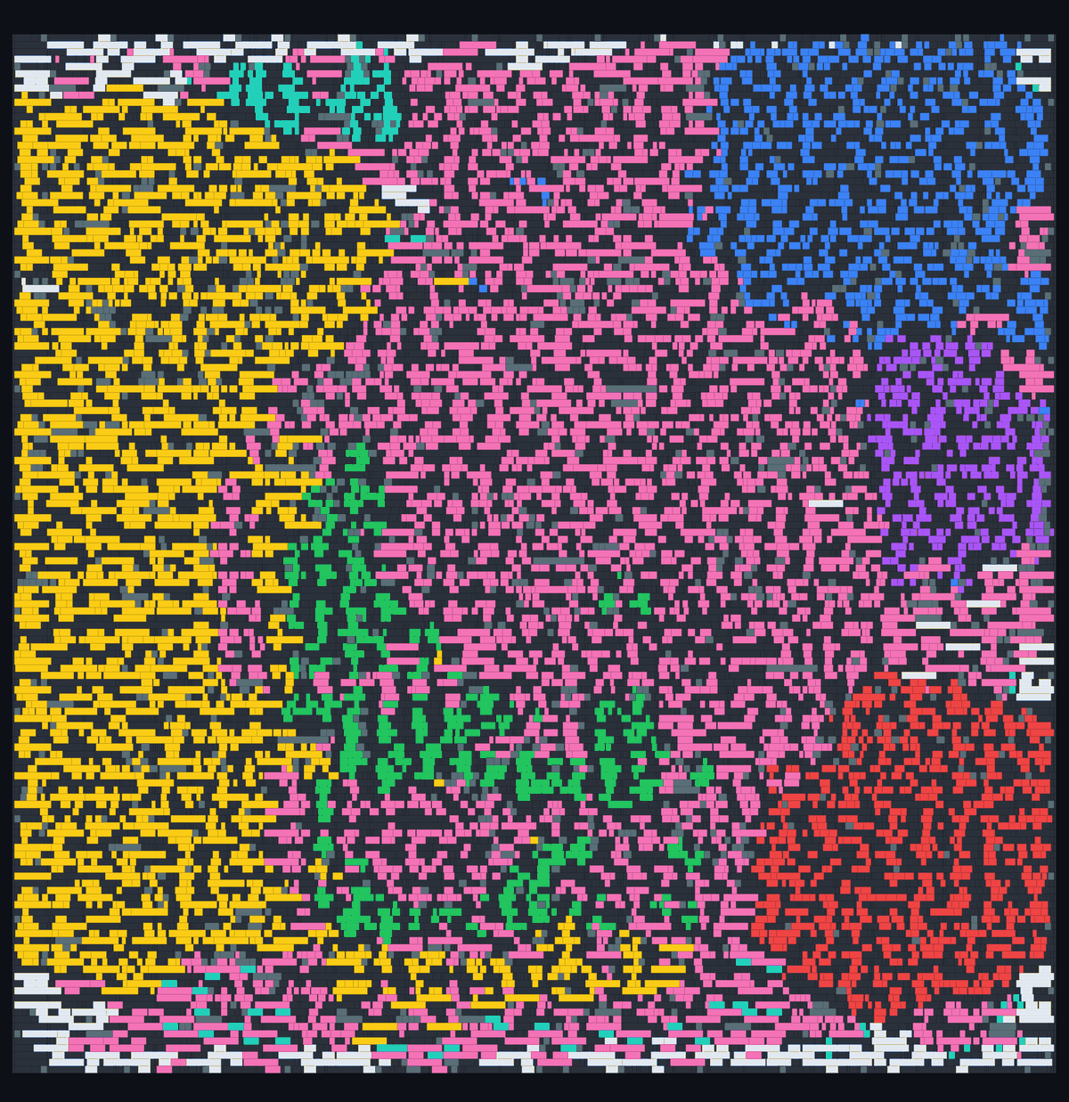
The core as a chip: z80_top, hardened on its own, as a hard macro in a ring of I/O pads, each pin's pad on the side of the die where the Z80 has its own. The layout shows the metal stack, bottom metal blue to top metal yellow; the clock and power picture the clock in green -- the CLK pad, every clock wire and buffer -- over the power rings, stripes and rails (core supply red, ground blue; a split I/O supply amber and teal) and the supply pads in their net's colour; the block map every cell by the Z80 block it was synthesized in. Where a chip has been simulated at transistor level -- its layout extracted to transistors and wires and run in ngspice (asic/spice) -- its pins are shown under it as a logic analyser shows them.

IHP SG13G2 chip, 48 pads: layout
layout
IHP SG13G2 chip, 48 pads: clock and power
clock and power
IHP SG13G2 chip, 48 pads: cells by Z80 block
cells by Z80 block

IHP SG13G2 chip, 48 pads

ihp-sg13g2 · sg13g2_stdcell

Die
1,600 × 1,600 µm (2.56 mm²)
Pads
48, each on the side of the Z80's own
Clock
4 MHz, setup slack +26.43 ns (typical)

Clock and power

  • clock: CLK pad, wires, buffers 89
  • core supply (VDD) 2
  • ground (VSS) 2
  • I/O supply (IOVDD) 3
  • I/O ground (IOVSS) 3
  • signal pads 37

Cells by Z80 block

  • I/O pads 48
  • ALU 460
  • register file 1,192
  • decoder PLA 230
  • execute 513
  • address 322
  • timing 130
  • core sequencer, state 2,090
  • pin logic 211
  • P&R buffers, clock tree 1,543
GlobalFoundries GF180MCU chip, 40 pads: layout
layout
GlobalFoundries GF180MCU chip, 40 pads: clock and power
clock and power
GlobalFoundries GF180MCU chip, 40 pads: cells by Z80 block
cells by Z80 block
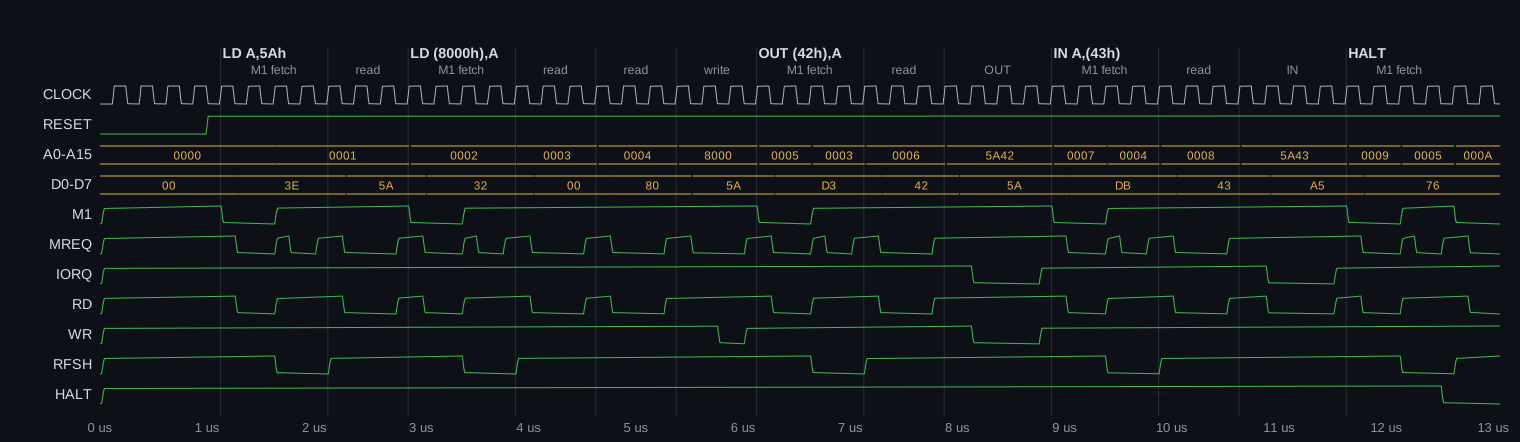
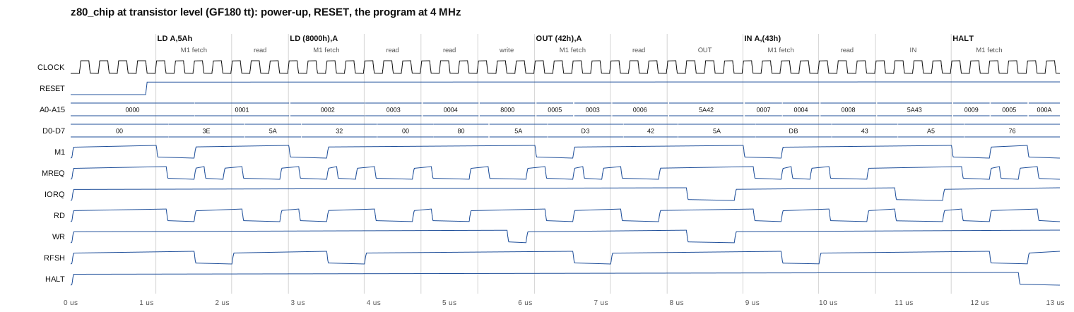
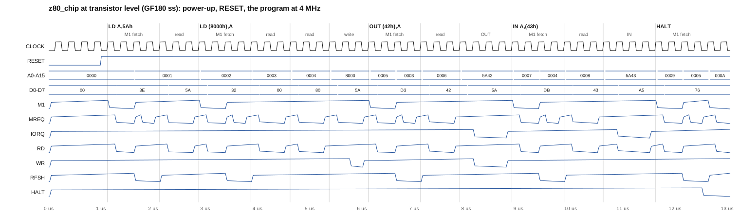
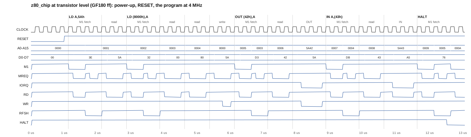
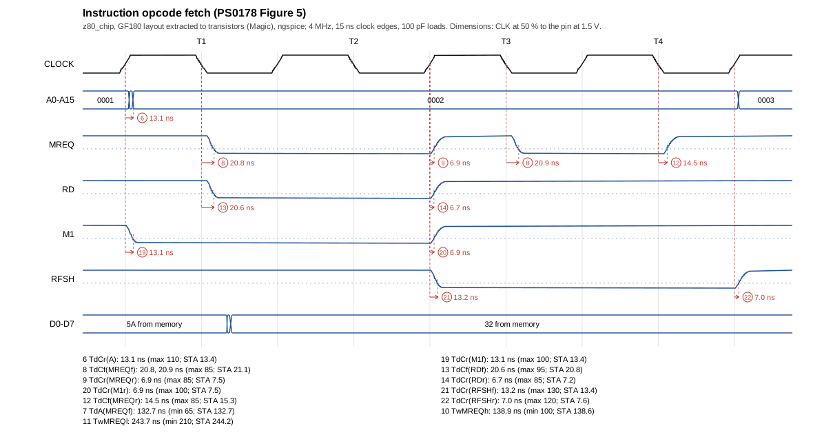
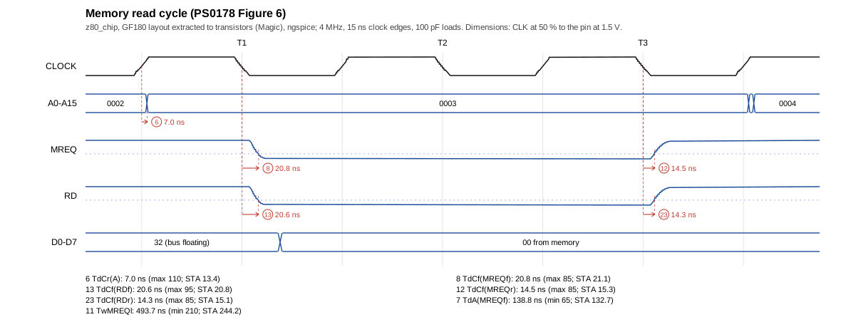
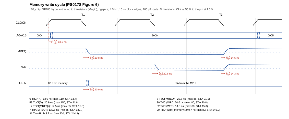
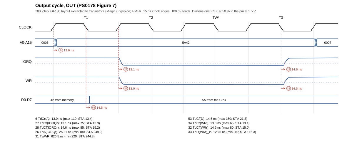
GlobalFoundries GF180MCU chip, 40 pads: its pins at transistor level (ngspice): power-up, RESET, a short program at 4 MHz
its pins at transistor level (ngspice): power-up, RESET, a short program at 4 MHz

GlobalFoundries GF180MCU chip, 40 pads

gf180mcuD · gf180mcu_fd_sc_mcu7t5v0

Die
1,662 × 1,512 µm (2.51 mm²)
Pads
40, each on the side of the Z80's own
Clock
4 MHz, setup slack +17.22 ns (typical)

Clock and power

  • clock: CLK pad, wires, buffers 72
  • core supply (VDD) 1
  • ground (VSS) 1
  • signal pads 37

Cells by Z80 block

  • I/O pads 40
  • ALU 595
  • register file 1,391
  • decoder PLA 284
  • execute 655
  • address 462
  • timing 144
  • core sequencer, state 2,801
  • pin logic 202
  • P&R buffers, clock tree 1,124
GlobalFoundries GF180MCU, 9-track cells chip, 40 pads: layout
layout
GlobalFoundries GF180MCU, 9-track cells chip, 40 pads: clock and power
clock and power
GlobalFoundries GF180MCU, 9-track cells chip, 40 pads: cells by Z80 block
cells by Z80 block

GlobalFoundries GF180MCU, 9-track cells chip, 40 pads

gf180mcuD · gf180mcu_fd_sc_mcu9t5v0

Die
1,662 × 1,512 µm (2.51 mm²)
Pads
40, each on the side of the Z80's own
Clock
4 MHz, setup slack +15.79 ns (typical)

Clock and power

  • clock: CLK pad, wires, buffers 48
  • core supply (VDD) 1
  • ground (VSS) 1
  • signal pads 37

Cells by Z80 block

  • I/O pads 40
  • ALU 590
  • register file 1,409
  • decoder PLA 280
  • execute 646
  • address 494
  • timing 148
  • core sequencer, state 2,848
  • pin logic 202
  • P&R buffers, clock tree 925

At transistor level

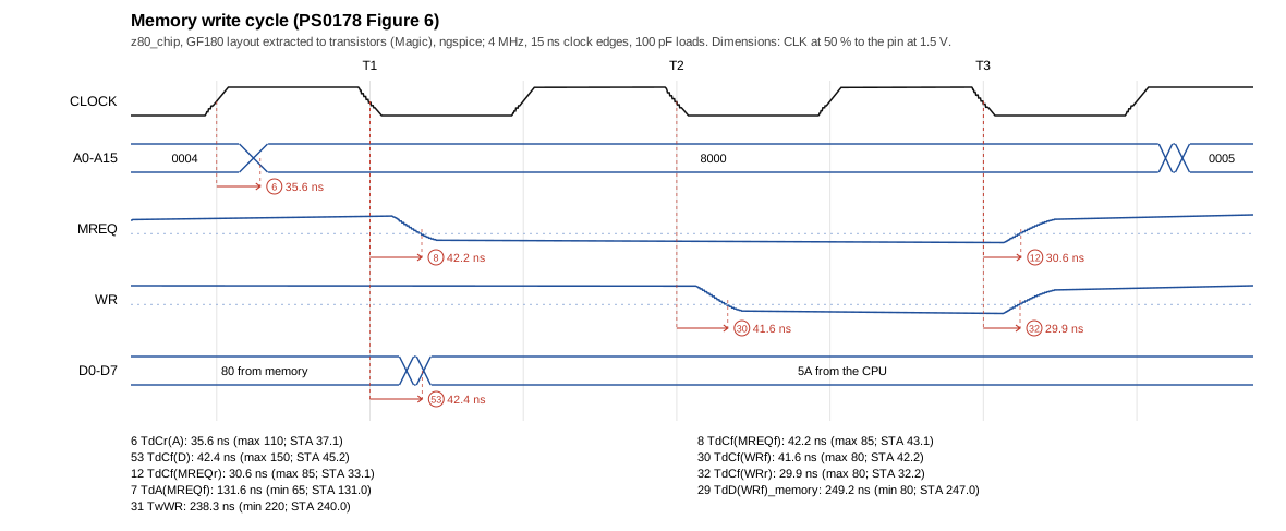
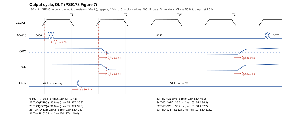
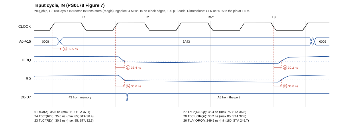
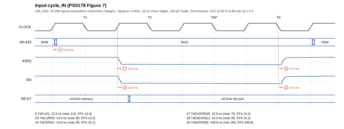
The timing above is OpenSTA's, from the PDKs' Liberty models. Here the chips run as transistors, in ngspice with the PDKs' own netlists and transistor models, against the NMOS Z80 datasheet's test conditions (asic/spice).

The whole chip, GlobalFoundries GF180MCU

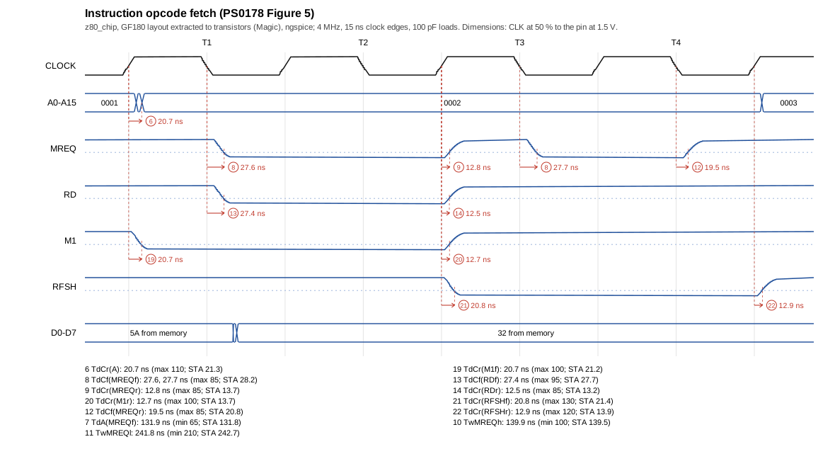
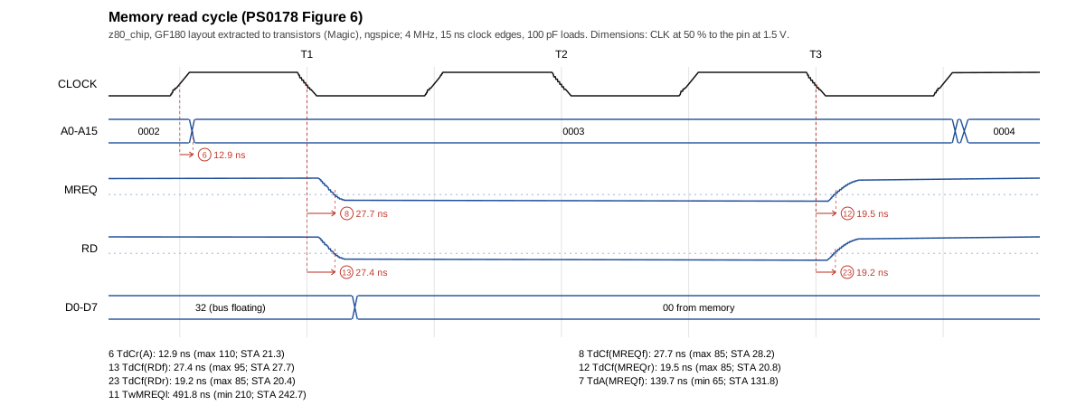
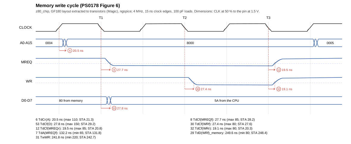
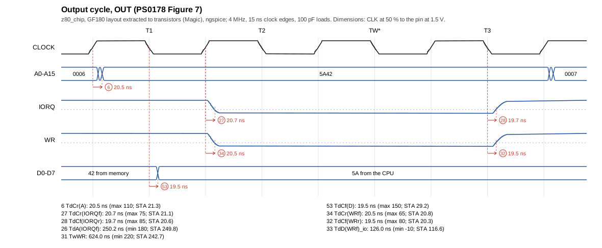
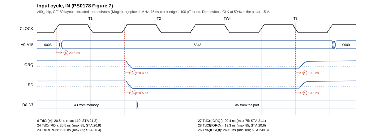
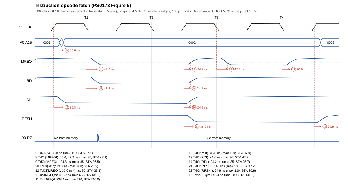
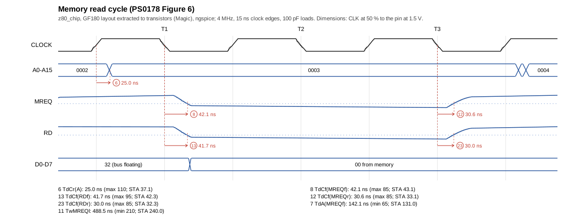
The chip's layout extracted with Magic to its transistors and their wiring, and run in ngspice at each corner (tt, ss, ff): power-up, RESET, and a short program -- a memory read, a memory write, an I/O write and read -- at 4 MHz with 15 ns edges, its outputs into 100 pF (chip.py; hours, so run now and then and committed). Its pins are checked against the RTL at every clock edge after RESET, and the cycles measured as the Z80 manual draws them; the figures below are each corner's: the switch over them changes the corner in place, the dimensions too.

CornerPins against the RTL: mismatchesAC parameters met Closest to its limitFigures
tt025 of 2521.8 ns TwWRprogram · opcode fetch (M1) · memory read · memory write · I/O write · I/O read
ss025 of 2518.3 ns TwWRprogram · opcode fetch (M1) · memory read · memory write · I/O write · I/O read
ff025 of 2523.7 ns TwWRprogram · opcode fetch (M1) · memory read · memory write · I/O write · I/O read
The datasheet's AC parameters: 25 of 25 met at every corner, over every cycle that has them
#ParameterLimittt: SPICE (cycles)ss: SPICE (cycles)ff: SPICE (cycles)
6TdCr(A)≤ 110 ns12.9 – 20.7 ns (15) STA 21.325.0 – 35.9 ns (15) STA 37.17.0 – 13.1 ns (15) STA 13.4
7TdA(MREQf)≥ 65 ns131.9 – 139.7 ns (9) STA 131.8131.2 – 142.1 ns (9) STA 131.0132.7 – 138.8 ns (9) STA 132.7
8TdCf(MREQf)≤ 85 ns27.6 – 27.7 ns (16) STA 28.242.0 – 42.2 ns (16) STA 43.120.8 – 20.9 ns (16) STA 21.1
9TdCr(MREQr)≤ 85 ns12.7 – 12.8 ns (5) STA 13.724.6 – 24.8 ns (5) STA 26.56.9 – 6.9 ns (5) STA 7.5
10TwMREQh≥ 100 ns139.9 – 139.9 ns (5) STA 139.5142.4 – 142.4 ns (5) STA 141.6138.9 – 138.9 ns (5) STA 138.6
11TwMREQl≥ 210 ns241.8 – 492.3 ns (10) STA 242.7238.4 – 489.3 ns (10) STA 240.0243.7 – 494.0 ns (10) STA 244.2
12TdCf(MREQr)≤ 85 ns19.5 – 19.9 ns (11) STA 20.830.6 – 31.4 ns (11) STA 33.114.5 – 14.8 ns (11) STA 15.3
13TdCf(RDf)≤ 95 ns27.4 – 27.4 ns (10) STA 27.741.6 – 41.7 ns (10) STA 42.320.6 – 20.6 ns (10) STA 20.8
14TdCr(RDr)≤ 85 ns12.4 – 12.5 ns (5) STA 13.224.1 – 24.2 ns (5) STA 25.76.7 – 6.7 ns (5) STA 7.2
19TdCr(M1f)≤ 100 ns20.7 – 20.7 ns (5) STA 21.235.8 – 35.9 ns (5) STA 37.013.1 – 13.1 ns (5) STA 13.4
20TdCr(M1r)≤ 100 ns12.7 – 12.7 ns (5) STA 13.724.7 – 24.7 ns (5) STA 26.56.9 – 6.9 ns (5) STA 7.5
21TdCr(RFSHf)≤ 130 ns20.8 – 20.8 ns (5) STA 21.436.0 – 36.0 ns (5) STA 37.213.1 – 13.2 ns (5) STA 13.4
22TdCr(RFSHr)≤ 120 ns12.9 – 12.9 ns (5) STA 13.924.9 – 24.9 ns (5) STA 26.97.0 – 7.0 ns (5) STA 7.6
23TdCf(RDr)≤ 85 ns19.2 – 19.6 ns (6) STA 20.430.0 – 30.8 ns (6) STA 32.314.3 – 14.6 ns (6) STA 15.1
24TdCr(RDf)≤ 85 ns20.5 – 20.5 ns (1) STA 20.935.6 – 35.6 ns (1) STA 36.413.0 – 13.0 ns (1) STA 13.2
26TdA(IORQf)≥ 180 ns249.9 – 250.2 ns (2) STA 249.8249.9 – 250.2 ns (2) STA 249.7249.9 – 250.1 ns (2) STA 249.9
27TdCr(IORQf)≤ 75 ns20.4 – 20.7 ns (2) STA 21.135.4 – 35.8 ns (2) STA 36.812.9 – 13.1 ns (2) STA 13.3
28TdCf(IORQr)≤ 85 ns19.3 – 19.7 ns (2) STA 20.630.2 – 31.0 ns (2) STA 32.814.4 – 14.6 ns (2) STA 15.2
29TdD(WRf)_memory≥ 80 ns249.6 – 249.6 ns (1) STA 248.4249.2 – 249.2 ns (1) STA 247.0249.7 – 249.7 ns (1) STA 249.0
30TdCf(WRf)≤ 80 ns27.4 – 27.4 ns (1) STA 27.641.6 – 41.6 ns (1) STA 42.220.6 – 20.6 ns (1) STA 20.8
31TwWR≥ 220 ns241.8 – 624.0 ns (2) STA 242.7238.3 – 620.1 ns (2) STA 240.0243.7 – 626.5 ns (2) STA 244.3
32TdCf(WRr)≤ 80 ns19.1 – 19.5 ns (2) STA 20.329.9 – 30.7 ns (2) STA 32.214.3 – 14.5 ns (2) STA 15.0
33TdD(WRf)_io≥ -10 ns126.0 – 126.0 ns (1) STA 116.6129.9 – 129.9 ns (1) STA 116.0123.5 – 123.5 ns (1) STA 116.3
34TdCr(WRf)≤ 65 ns20.5 – 20.5 ns (1) STA 20.835.6 – 35.6 ns (1) STA 36.313.0 – 13.0 ns (1) STA 13.1
53TdCf(D)≤ 150 ns19.5 – 27.8 ns (2) STA 29.230.6 – 42.4 ns (2) STA 45.214.5 – 20.9 ns (2) STA 21.8
power-up, RESET, and the program at 4 MHz
power-up, RESET, and the program at 4 MHz, tt
opcode fetch (M1)
opcode fetch (M1), tt
memory read
memory read, tt
memory write
memory write, tt
I/O write
I/O write, tt
I/O read
I/O read, tt

The run on GitHub's runners, every corner's figures: transistor/ (transistor.yml, by hand).

The NMI pulse catcher

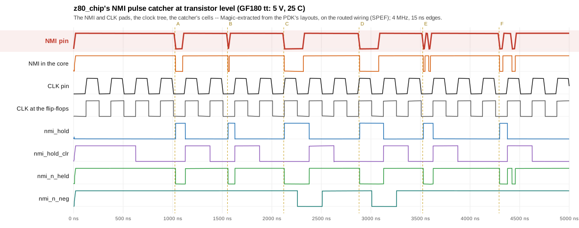
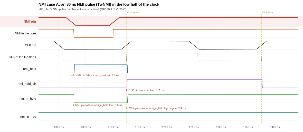
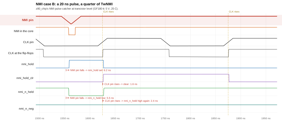
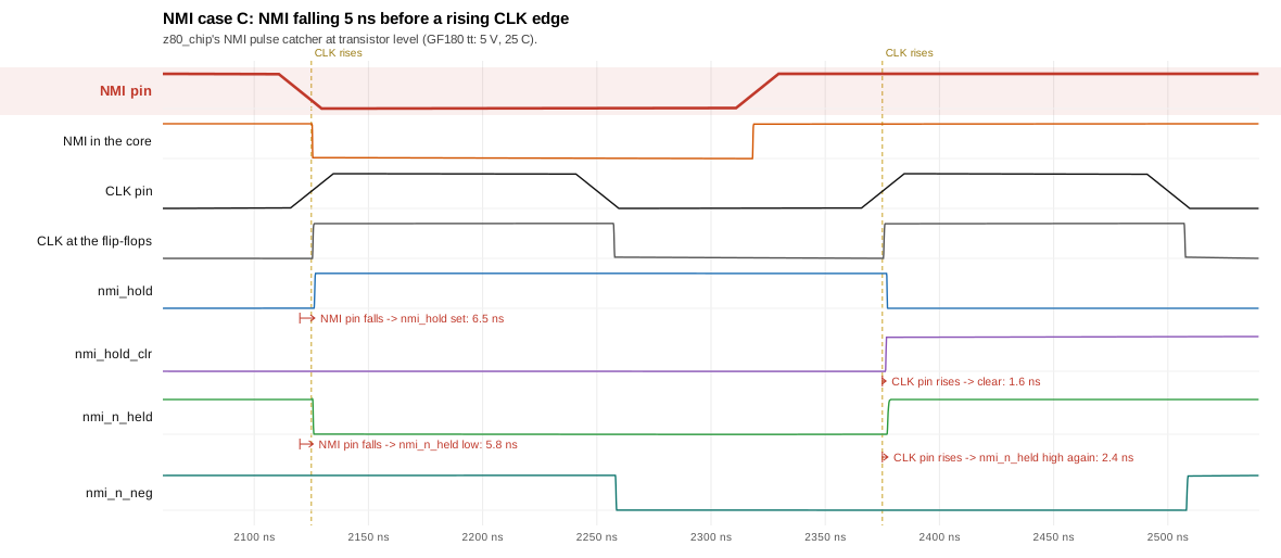
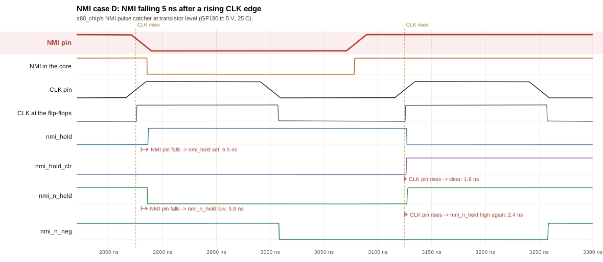
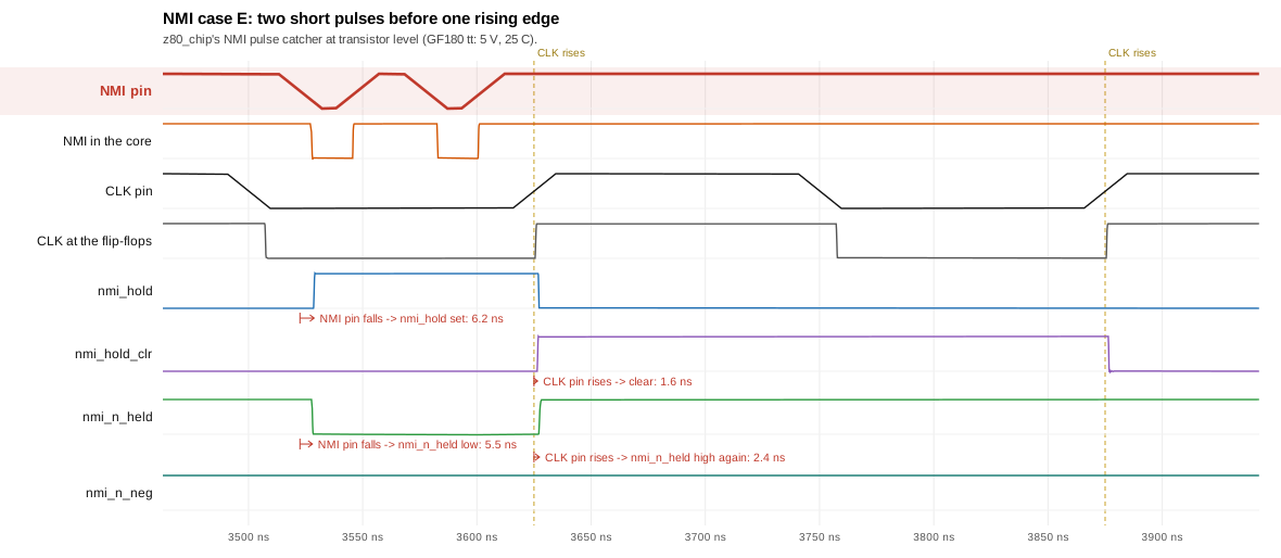
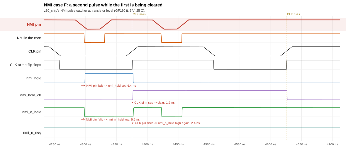
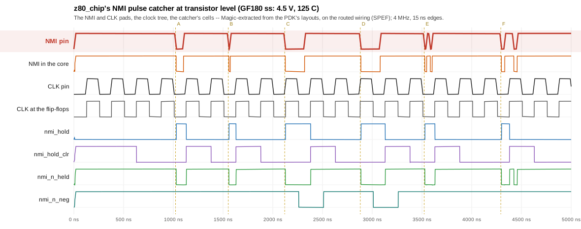
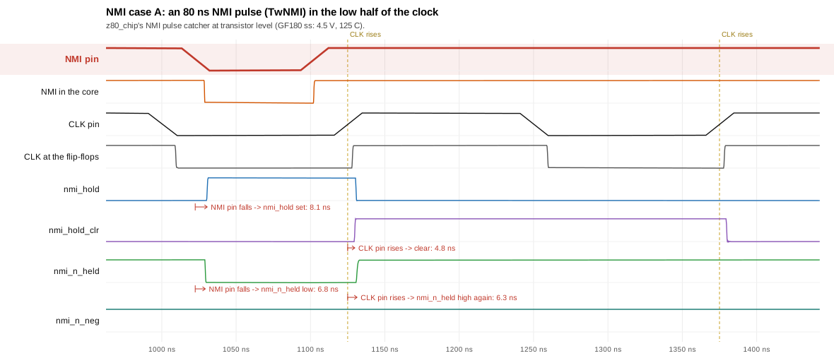
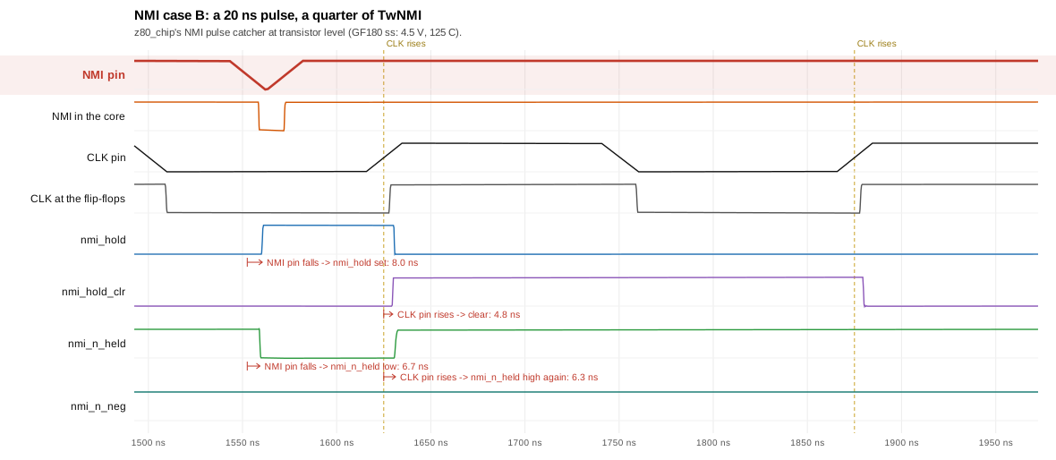
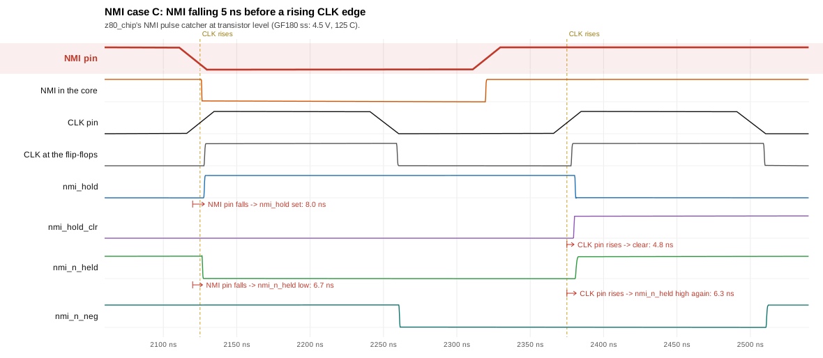
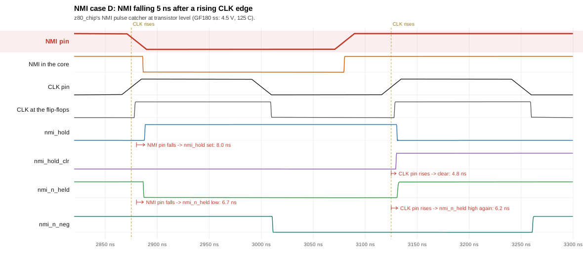
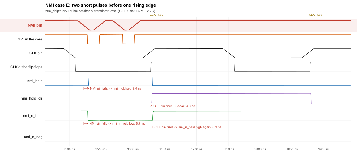
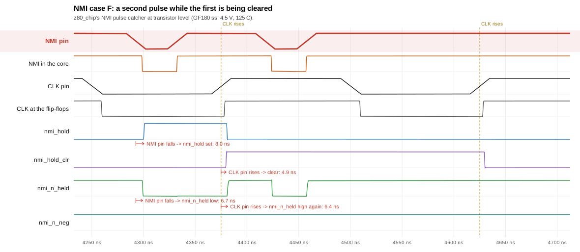
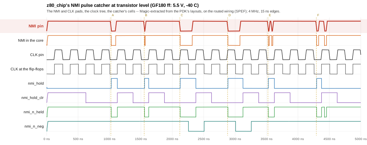
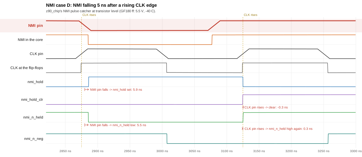
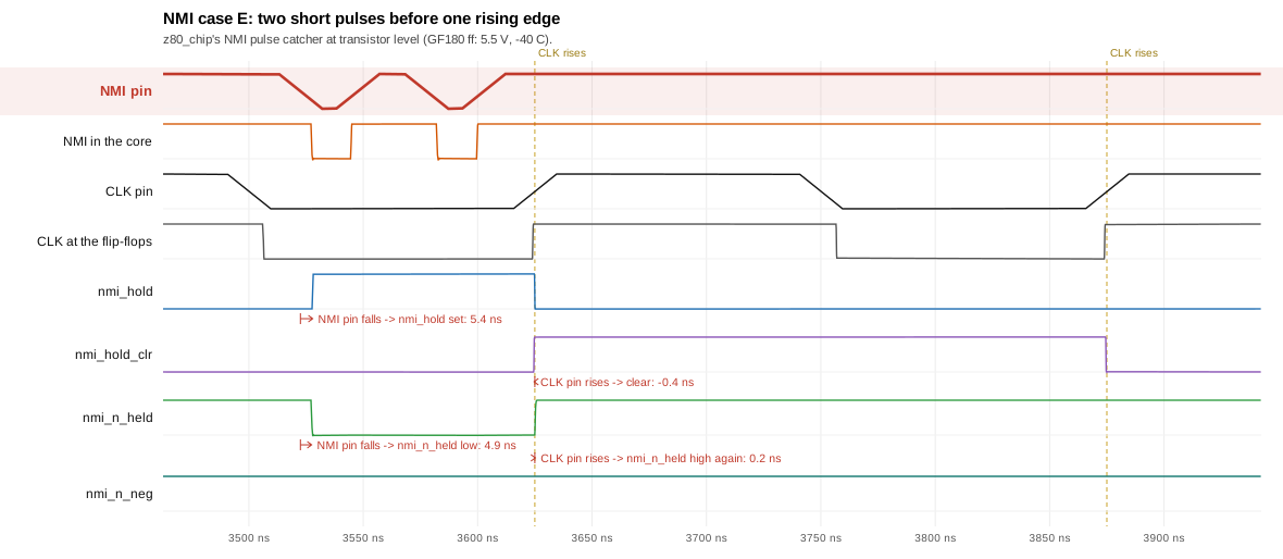
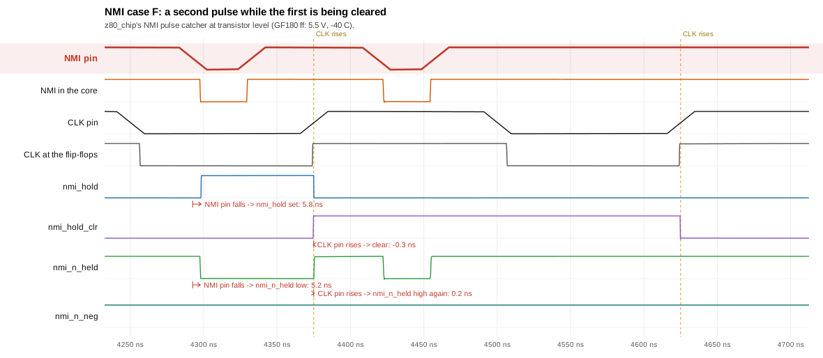
The NMOS Z80 takes an NMI pulse of any width -- TwNMI, 80 ns at 4 MHz, is under half a clock -- not only one a clock edge sees: a flip-flop clocked by the NMI pin itself catches it and holds it for the core until the next rising CLK edge, which clears it (z80_top.v). Here it is cut out of the GF180 7-track chip, from the NMI and CLK pins to the flip-flops -- the pads, the clock tree to its leaf, the cells as Magic extracts them from the PDK's layouts, on the routed chip's wiring -- and run at each corner with six pulses (nmi.py).

CornerPulses caught and clearedNMI pin falls → caught (A) CLK pin rises → cleared (A)The core sees NMI for (A)Figures
tt 5.0 V, 25 °C6 of 66.4 ns1.6 ns99.3 nsall · A · B · C · D · E · F
ss 4.5 V, 125 °C6 of 68.1 ns4.8 ns102.0 nsall · A · B · C · D · E · F
ff 5.5 V, -40 °C6 of 65.4 ns-0.3 ns97.8 nsall · A · B · C · D · E · F
the six cases
the six cases, tt
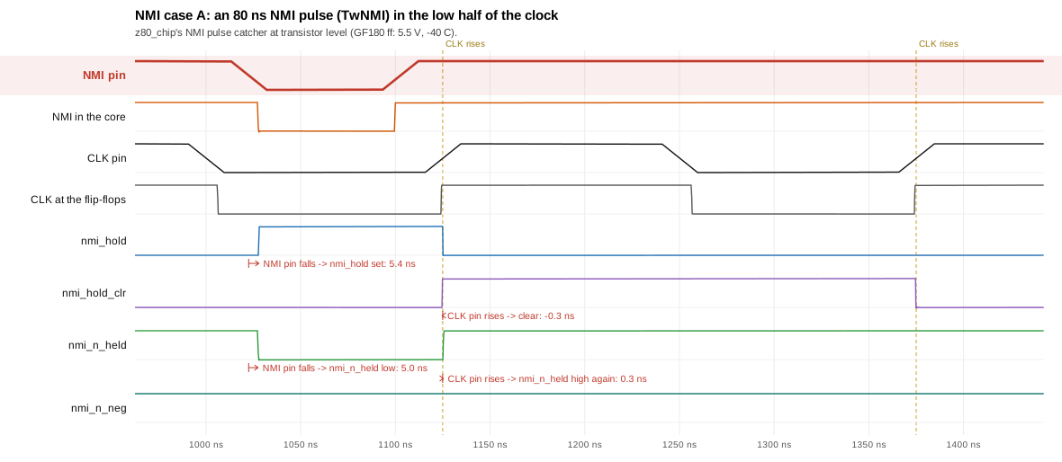
A: an 80 ns NMI pulse (TwNMI) in the low half of the clock
A: an 80 ns NMI pulse (TwNMI) in the low half of the clock, tt
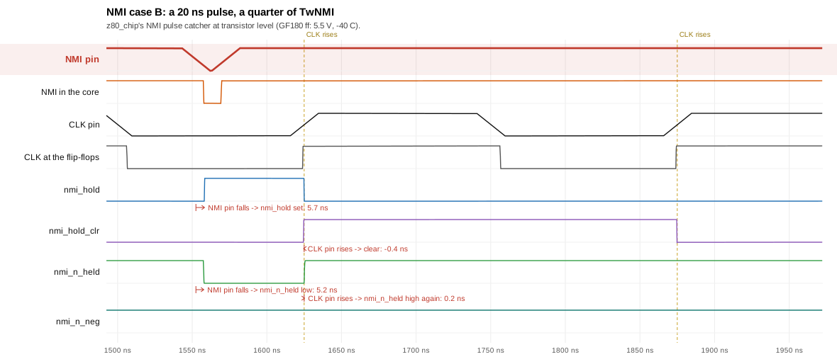
B: a 20 ns pulse, a quarter of TwNMI
B: a 20 ns pulse, a quarter of TwNMI, tt
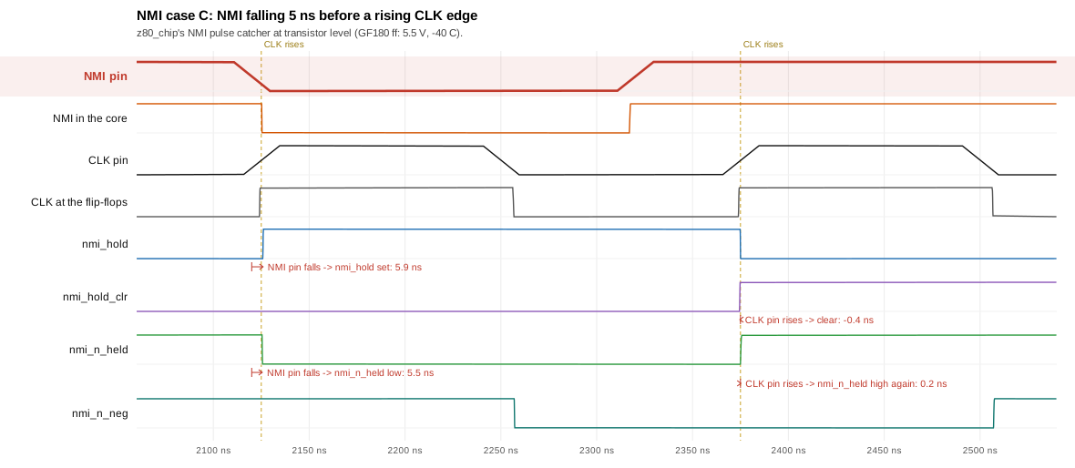
C: NMI falling 5 ns before a rising CLK edge
C: NMI falling 5 ns before a rising CLK edge, tt
D: NMI falling 5 ns after a rising CLK edge
D: NMI falling 5 ns after a rising CLK edge, tt
E: two short pulses before one rising edge
E: two short pulses before one rising edge, tt
F: a second pulse while the first is being cleared
F: a second pulse while the first is being cleared, tt

The pads

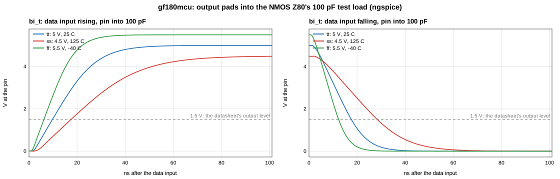
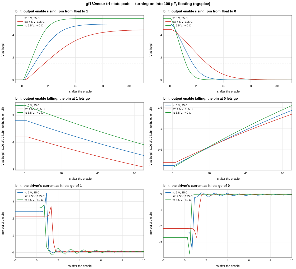
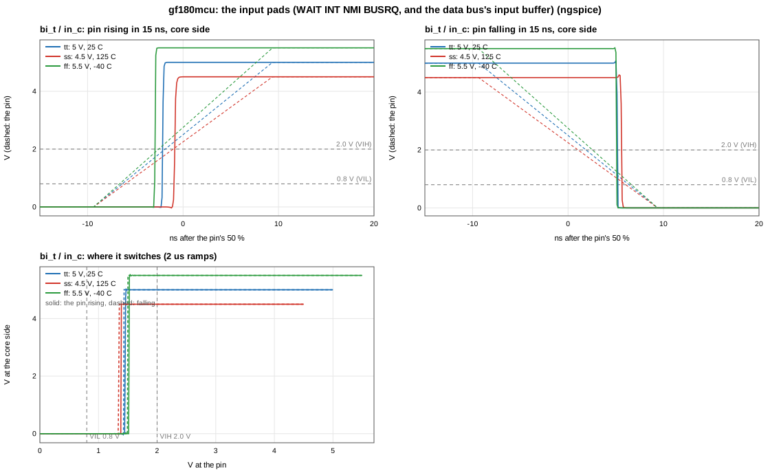
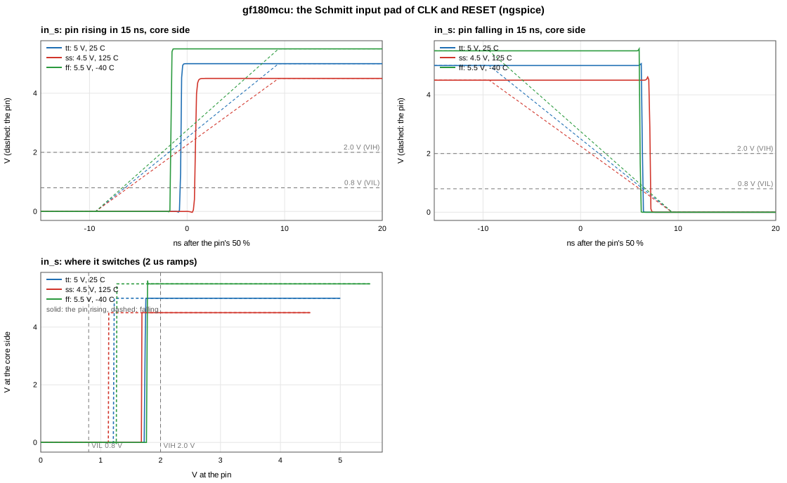
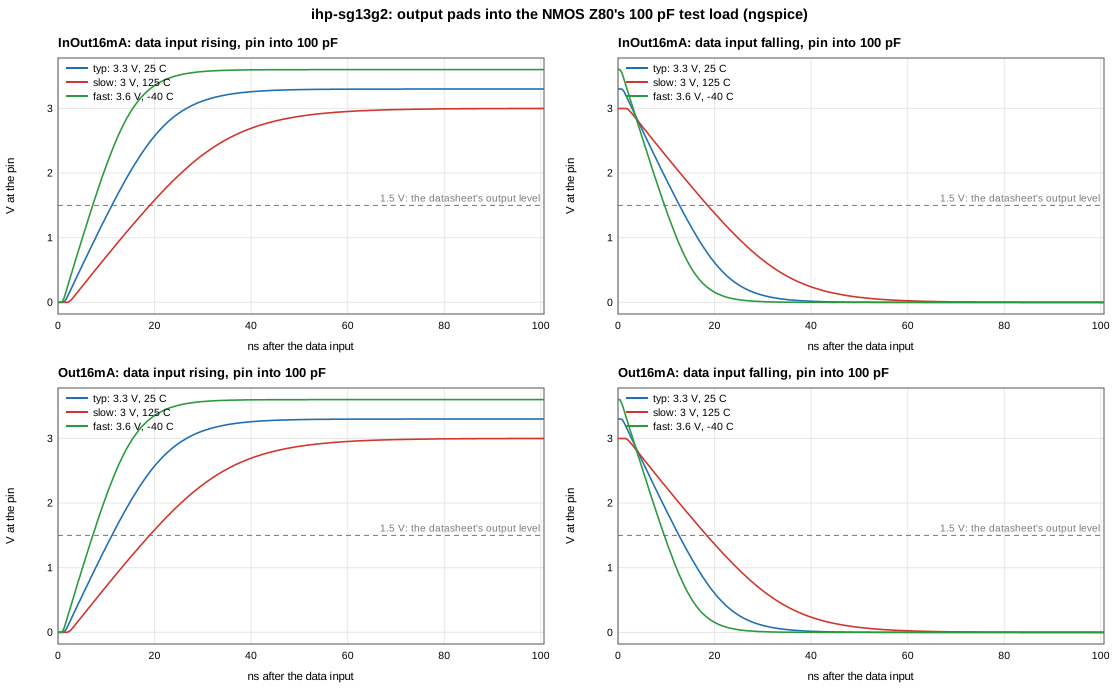
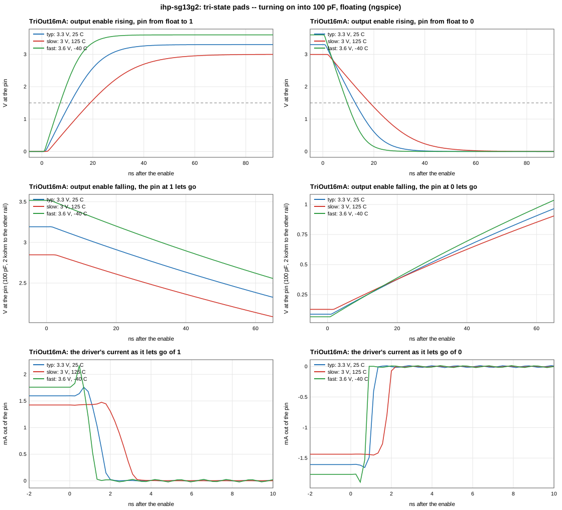
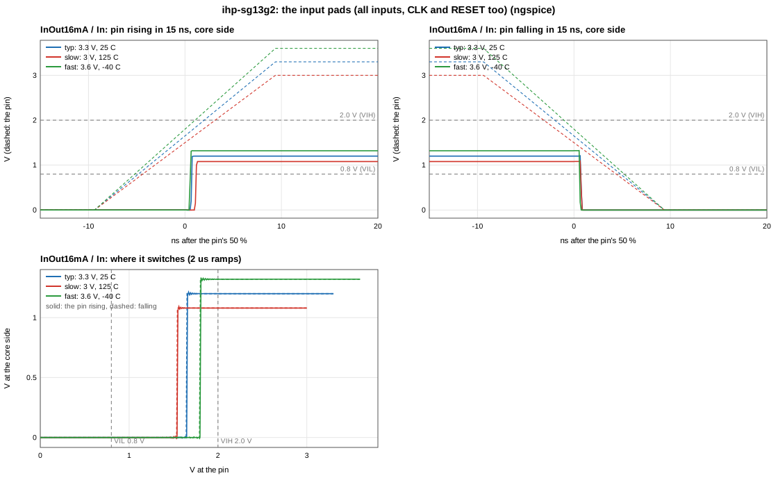
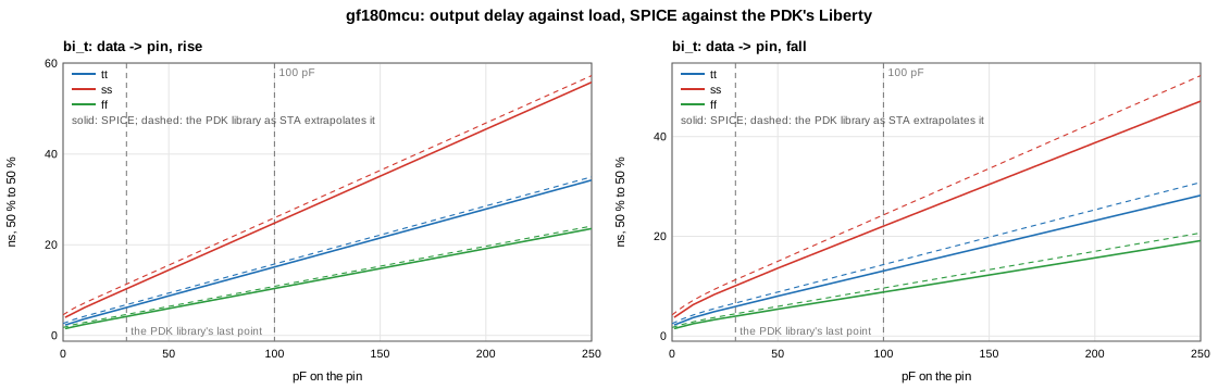
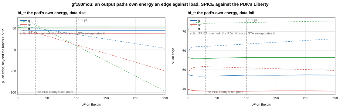
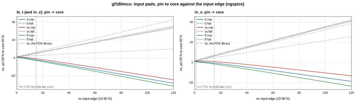
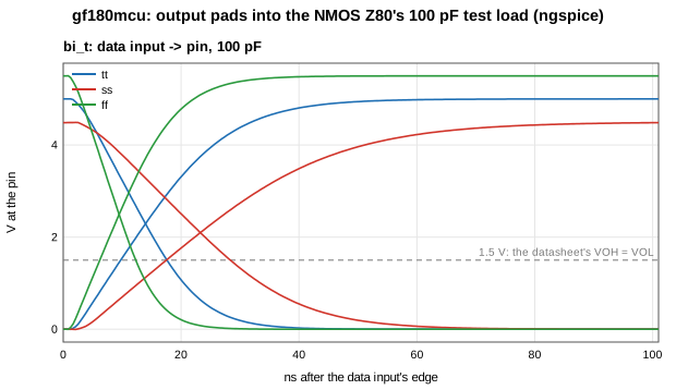
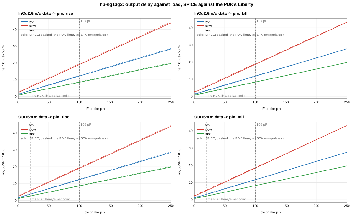
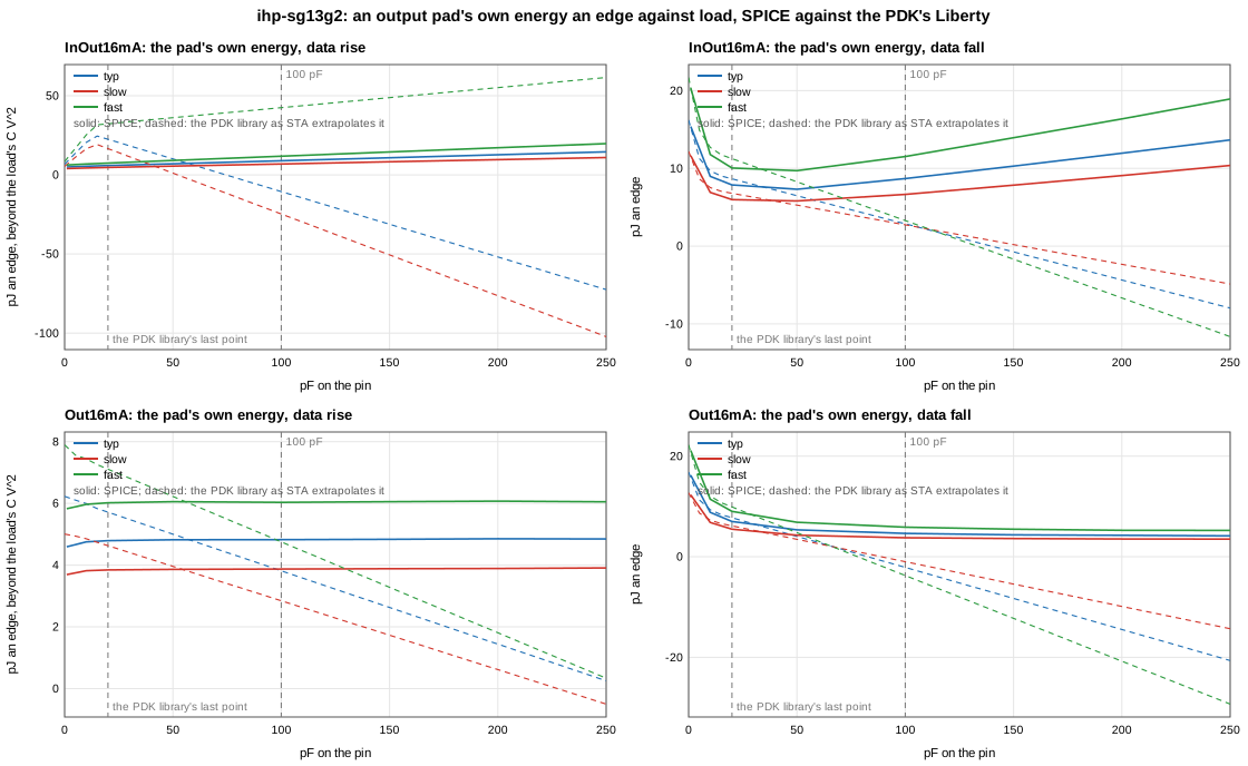
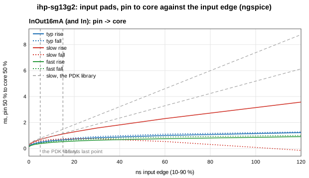
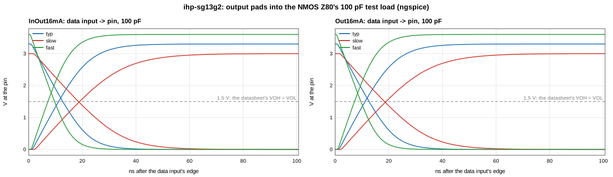
Every pad cell the chips use, from the PDK's own netlist with its transistor models, at the corners the chips are signed off at (pads.py): the outputs into 1–250 pF, the data bus's tri-state pads turning on and floating, the inputs on edges up to 120 ns, and the Schmitt-trigger input CLK and RESET take. Checked in every run against the committed results; their Liberty files replace the PDKs' own in the chips' pin-timing checks (pin_timing.py).

GF180 gf180mcu_fd_io's 5 V pads · summary · delay vs load · energy vs load · inputs vs edge · waveforms · pads.json · Liberty: ff_n40C_5v50, ss_125C_4v50, tt_025C_5v00

outputs: edges into 1–250 pF, and their drive
the data bus: turning on, and floating
inputs: pin to core on edges up to 120 ns, and where they switch
CLK and RESET: the Schmitt-trigger input

IHP SG13G2 sg13g2_io's 3.3 V pads · summary · delay vs load · energy vs load · inputs vs edge · waveforms · pads.json · Liberty: fast_1p32V_3p6V_m40C, slow_1p08V_3p0V_125C, typ_1p2V_3p3V_25C

outputs: edges into 1–250 pF, and their drive
the data bus: turning on, and floating
inputs: pin to core on edges up to 120 ns, and where they switch

ASIC core layouts

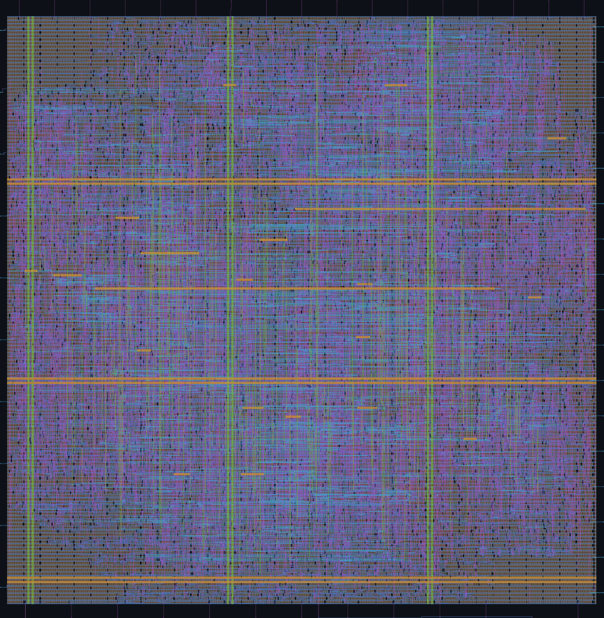
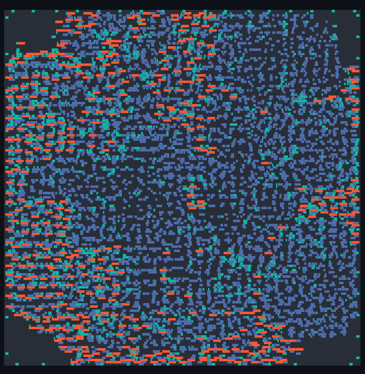
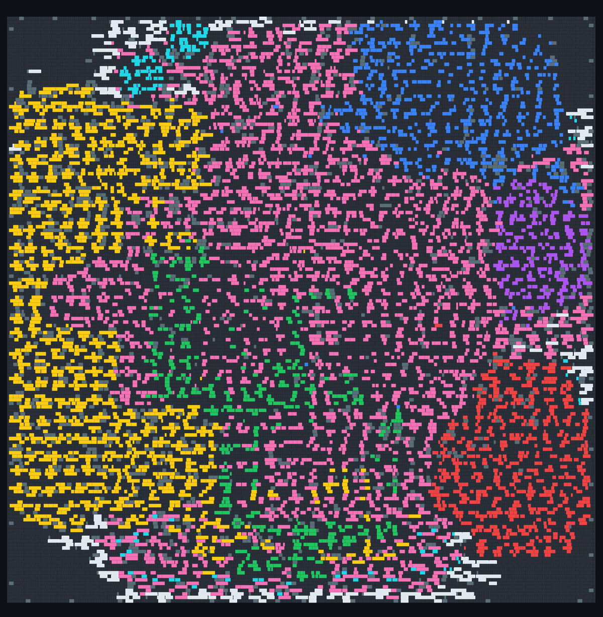
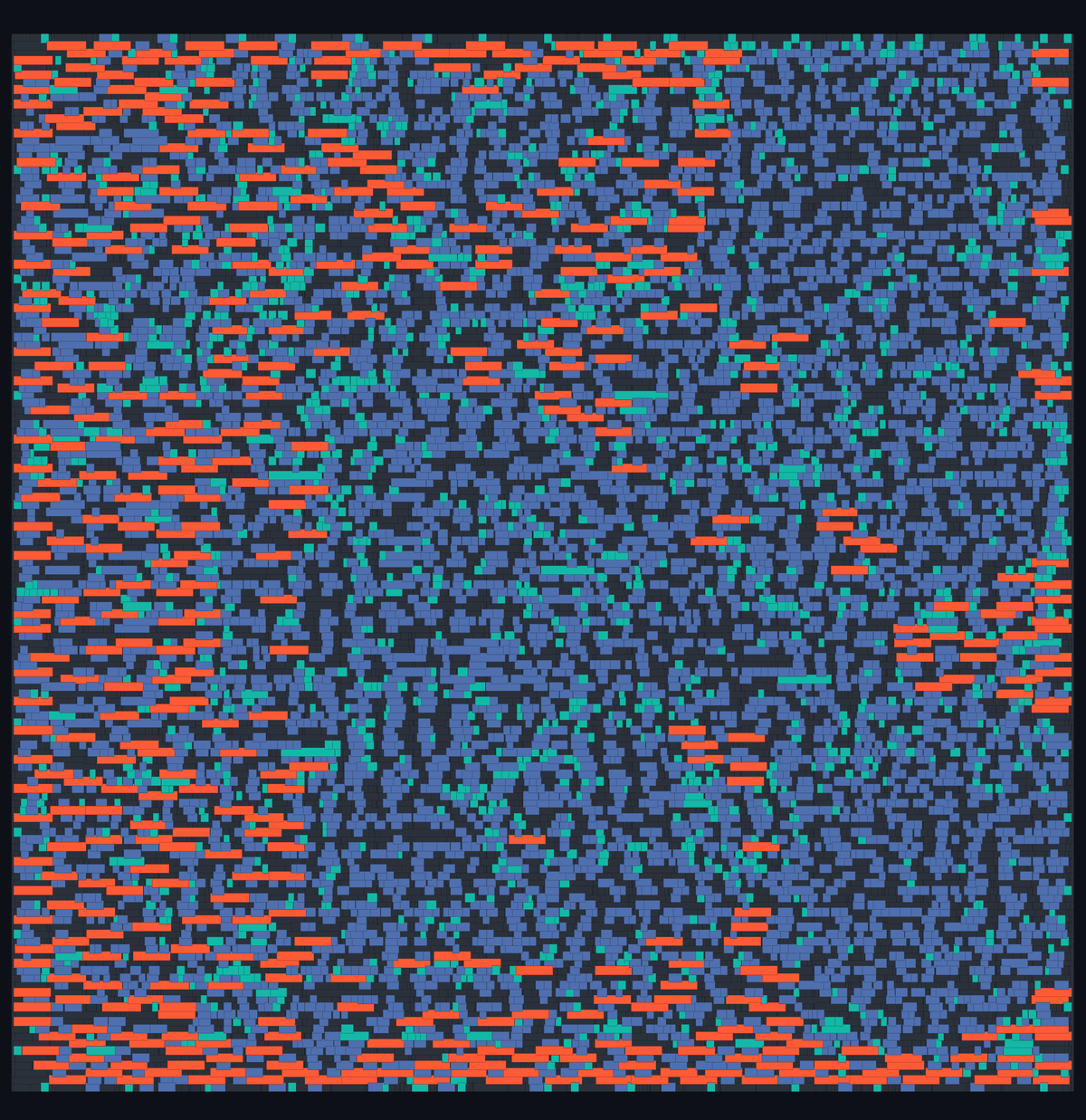
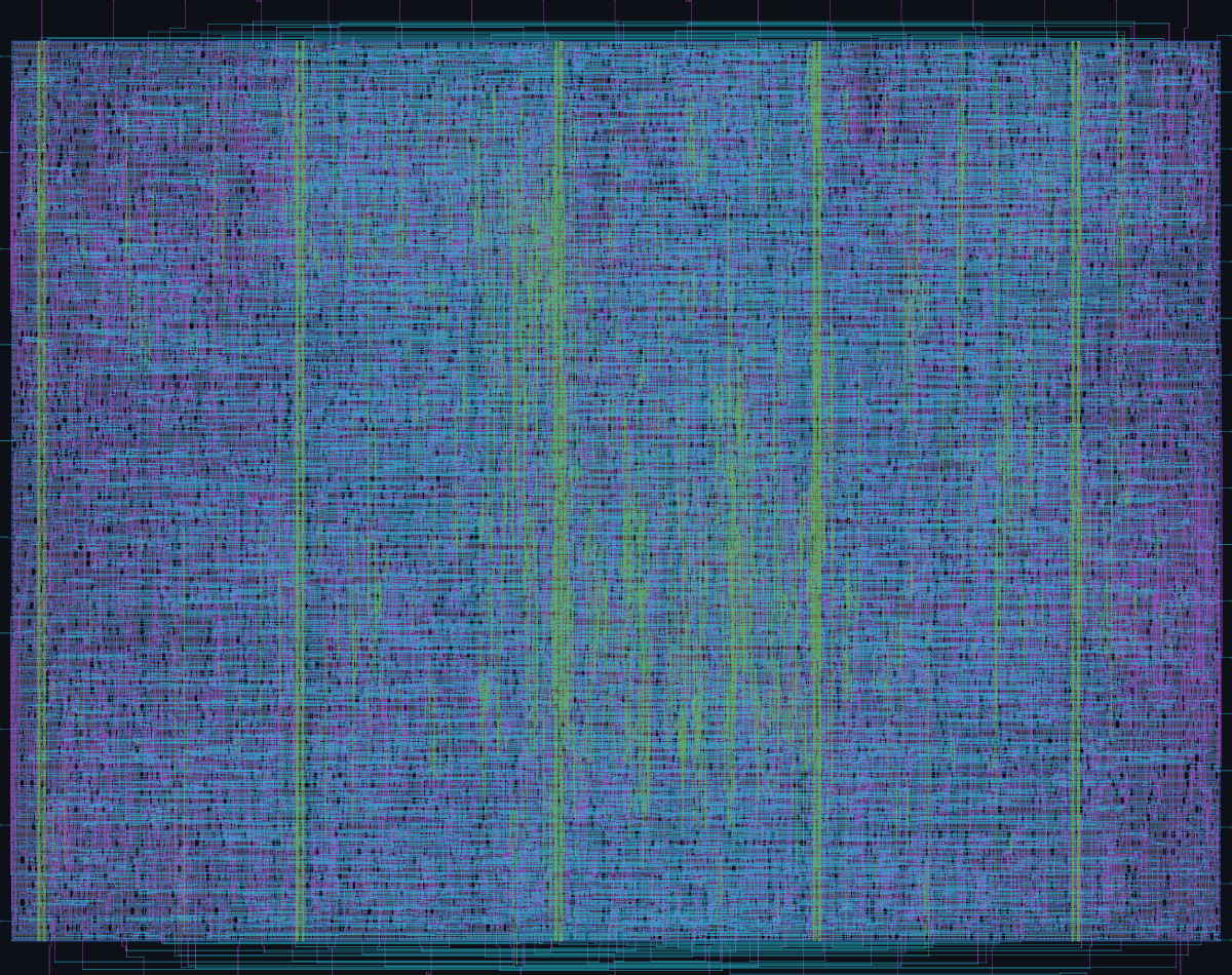
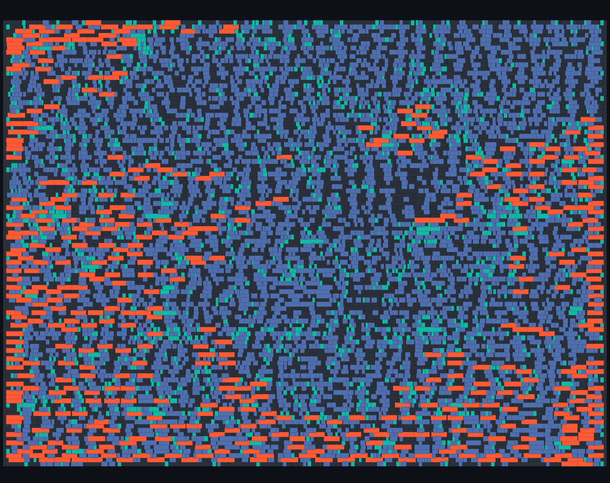
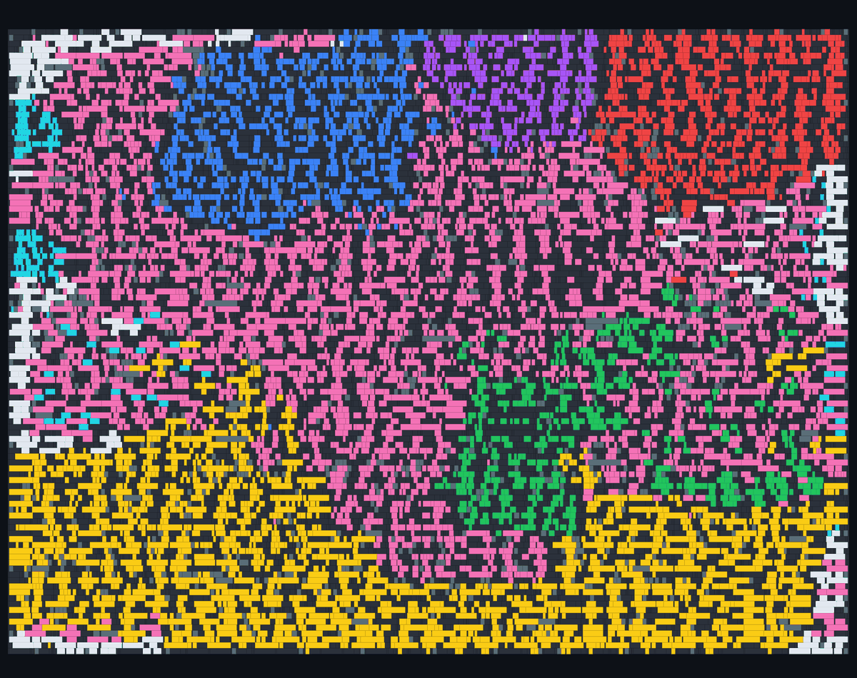
The bare core (no pad ring), RTL to GDS with LibreLane. The pictures are drawn from the GDS and the DEF: the layout shows the cell rows and the metal stack, bottom metal blue to top metal yellow; the two cell maps show every standard cell, coloured by kind and by the Z80 block it was synthesized in.

SkyWater SKY130: layout
layout
SkyWater SKY130: cells by kind
cells by kind
SkyWater SKY130: cells by Z80 block
cells by Z80 block

SkyWater SKY130

sky130A · sky130_fd_sc_hd

Die
464 × 475 µm (0.22 mm²)
Std cells
10,012 (38 % utilisation)
Clock
20 MHz, setup slack +10.61 ns (typical)

Cells by kind

  • flip-flops 471
  • buffers and delays 1,494
  • logic 4,960
  • fill/decap/tap 39,430

Cells by Z80 block

  • ALU 561
  • register file 1,107
  • decoder PLA 255
  • execute 562
  • address 414
  • timing 134
  • core sequencer, state 2,413
  • pin logic 201
  • P&R buffers, clock tree 1,278
IHP SG13G2: layout
layout
IHP SG13G2: cells by kind
cells by kind
IHP SG13G2: cells by Z80 block
cells by Z80 block

IHP SG13G2

ihp-sg13g2 · sg13g2_stdcell

Die
452 × 471 µm (0.21 mm²)
Std cells
8,635 (54 % utilisation)
Clock
20 MHz, setup slack +11.89 ns (typical)

Cells by kind

  • flip-flops 471
  • buffers and delays 2,049
  • logic 74,312
  • fill/decap/tap 11,115

Cells by Z80 block

  • ALU 460
  • register file 1,192
  • decoder PLA 230
  • execute 513
  • address 322
  • timing 130
  • core sequencer, state 2,090
  • pin logic 211
  • P&R buffers, clock tree 1,529
GlobalFoundries GF180MCU: layout
layout
GlobalFoundries GF180MCU: cells by kind
cells by kind
GlobalFoundries GF180MCU: cells by Z80 block
cells by Z80 block

GlobalFoundries GF180MCU

gf180mcuD · gf180mcu_fd_sc_mcu7t5v0

Die
585 × 603 µm (0.35 mm²)
Std cells
10,062 (54 % utilisation)
Clock
20 MHz, setup slack +7.07 ns (typical)

Cells by kind

  • flip-flops 471
  • buffers and delays 1,503
  • logic 5,592
  • fill/decap/tap 15,282

Cells by Z80 block

  • ALU 595
  • register file 1,391
  • decoder PLA 284
  • execute 655
  • address 462
  • timing 144
  • core sequencer, state 2,801
  • pin logic 201
  • P&R buffers, clock tree 1,033
GlobalFoundries GF180MCU, 9-track cells: layout
layout
GlobalFoundries GF180MCU, 9-track cells: cells by kind
cells by kind
GlobalFoundries GF180MCU, 9-track cells: cells by Z80 block
cells by Z80 block

GlobalFoundries GF180MCU, 9-track cells

gf180mcuD · gf180mcu_fd_sc_mcu9t5v0

Die
732 × 579 µm (0.42 mm²)
Std cells
9,720 (56 % utilisation)
Clock
20 MHz, setup slack +6.05 ns (typical)

Cells by kind

  • flip-flops 471
  • buffers and delays 1,351
  • logic 5,659
  • fill/decap/tap 13,509

Cells by Z80 block

  • ALU 590
  • register file 1,409
  • decoder PLA 280
  • execute 646
  • address 494
  • timing 148
  • core sequencer, state 2,848
  • pin logic 201
  • P&R buffers, clock tree 865

FPGA bitstreams

BASIC computer: NASCOM BASIC 4.7 on the board's serial console. Tiny BASIC: the same computer with 1K Tiny BASIC. Chip: the board as a Z80 replacement, the bus on its pins. Each board's README says how to program it.

BoardBASIC computerTiny BASICZ80 chip replacement
IcePi Zero
Lattice ECP5 LFE5U-25F · README
.bit 250 KB.bit 249 KB.bit 168 KB
Sipeed Tang Primer 25K
Gowin GW5A-LV25MG121NES · README
.fs 6.8 MB.fs 6.8 MB.fs 5.9 MB
iCEBreaker
Lattice iCE40UP5K · README
.bin 104 KB.bin 104 KB.bin 104 KB
pico-ice
Lattice iCE40UP5K + RP2040 · README
.bin 104 KB
.uf2 208 KB
.bin 104 KB.bin 104 KB
.uf2 208 KB
iCESugar
Lattice iCE40UP5K · README
.bin 104 KB.bin 104 KB.bin 104 KB

The C model, for emulators

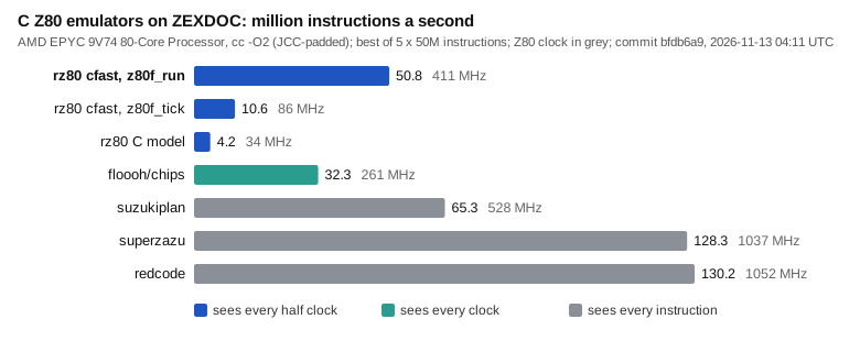
cfast is the C model generated into a phase engine: every half clock the same pins as the model and the RTL (make cfast_identity), at the speed an emulator needs. Here it runs against four other C Z80 emulators on the same 50 million ZEXDOC instructions, the best of 5 rounds of CPU time on GitHub's runner (AMD EPYC 9V74 80-Core Processor): the latest ci.yml run on main @ bfdb6a9, 2026-11-13 04:11 UTC. Every push runs it; how, and what the columns mean: cfast/BENCHMARK.md.

ZEXDOC million instructions a second, per emulator
EmulatorSees everyZEXDOC Minstr/sZ80 clockAgainst cfast What it is
rz80 cfast, z80f_runhalf clock50.8411 MHz1.00×the phase engine generated from the C model's timing tables, steps back to back with the bus inlined (cfast/)
rz80 cfast, z80f_tickhalf clock10.686 MHz0.21×the same steps, one half clock per call, the pins in a word
rz80 C modelhalf clock4.234 MHz0.08×the reference model the RTL is checked against (cmodel/)
floooh/chipsclock32.3261 MHz0.64×floooh/chips z80.h: z80_tick, the pins in a word
suzukiplaninstruction65.3528 MHz1.28×suzukiplan/z80: execute(1)
superzazuinstruction128.31037 MHz2.53×superzazu/z80: z80_step
redcodeinstruction130.21052 MHz2.56×redcode/Z80: z80_execute(1)